Six-channel Mixer and Amplifier
One of my most ambitious projects, this mixer was made for my friends Tony and Wilfred of
Mixed Fruit Jam as a practice amp. It's a relatively straightforward design, and will probably not be the best way of doing this. However, it works fairly well, and is relatively inexpensive to build.
Overview
The features list of this system are:
- Six independent microphone amplifiers with up to 60dB gain (theoretical, not tested). Each channel has an independent fader and an attenuator to allow connection of musical instruments which have line-level outputs (such as synthesizers).
- Mixer to combine all the six channels to a single monoaural output. This is available as the effects-send output (line out).
- Two stereo line-level inputs are provided, line-in (effects-receive) and aux-in. These are mixed together (no faders available, though), and sent to the next stage.
- Master volume and tone control, based on the National Semiconductor LM1036. This chip allows stereo volume and tone controls, without using expensive and unreliable ganged potentiometers.
- 68W RMS (tested up to 54W) per channel stereo power amplifier, based on the LM3886 monolithic power amplifier chip from National Semiconductor.
- Loudspeaker click-protection circuit and cooling fan controller with temperature-sensing diode.
- +/-30V DC power supply with a +/-15V regulated output.
Microphone Preamplifier
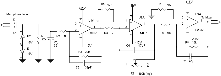
60 dB Microphone Preamp
The mike preamp itself is based on the LM837 Low-noise audio opamp from National Semiconductor. The first stage is a noninverting 26dB gain stage (fixed). Note the use of the 33pF capacitor in the feedback loop, this reduces the tendency of the LM837 to oscillate (it has a large bandwidth of 17MHz). Two 5.1V Zener diodes are connected back-to-back across the input, to protect the amplifier from large voltage transients at the input.
The next stage is an inverting variable gain stage (-∞ to 60dB), again with a 47pF capacitor across the gain-control resistor. The pot used here should be of high-quality to prevent crackling, etc. Also, the wires should be tightly twisted and shielded to prevent noise and mains-hum pickup. The last stage is an inverting buffer (unity gain), to correct the inversion caused by the variable gain stage.
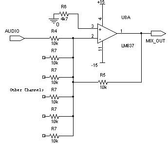
Mixer
The mixer itself is a fixed-gain summing amplifier based on an LM837. It sums up all the six microphone preamp signals into a single output. This is called the MIX OUT, and is a rear-panel socket. The single output is split into two outputs, to allow easy connection to external stereo equipment. The idea behind this is to allow connection of an external effects unit or graphic equalizer between the mixed output and the power amplifier.
Clipping Monitor
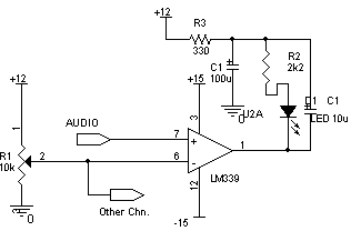
The clipping monitor is used to give a visual indication of when clipping occurs, in any of the input channels. The circuit shown is repeated for each channel. A potentiometer is used to select a clipping voltage to compare the inputs with, it should be adjusted to 2V. This will then give a clipping indication when the input crosses 2V, which would cause clipping in a line-level output. Of course, this does not mean that clipping wont occur at the final output, since the summed voltages from all the inputs can exceed 2V. The outputs of the LM339 are open-collector, so I've connected the output to the +12V supply, which is used only for the LEDs. This ensures that LED switching noise does not get into the power supply of the opamps. Note the use of a 10µF capactor across the LED, this gives a persistence effect to the LED, allowing the user to detect momentary clipping excursions. The 100µF/330Ω combination acts as an LPF, preventing switching currents from getting onto the supply line.
Input Mixer
The input mixer is a pair of 2-input mixers, similar to the six-input mixers shown above. These mix together the LINE-IN and AUX inputs, keeping the left/right inputs seperate. LINE-IN is meant for the effects-return line, while any external line-level inputs such as tape decks, computer audio outputs, etc. can be connected to the AUX-IN. The stereo output of the input mixers is given to the tone/volume/balance circuit.
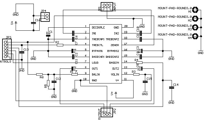
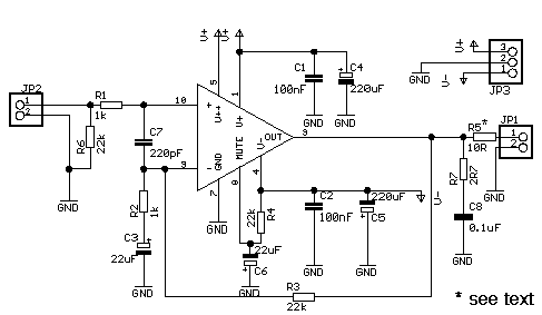
Tone/Volume/Balance
For simplicity, I've used the LM1036 tone/volume/balance chip to do this part of the mixer. The circuit is straight out of the
LM1036 datasheet. In my mixer, I disabled the balance input by using a pair of fixed resistors to give it a DC voltage of V
CC/2 Using the LM1036 may seem like laziness or a cop-out, but there's a good reason for using it: it's very difficult to get ganged pots, especially with a good match between channels. With the LM1036, you don't need ganged pots. The disadvantage is a reduction in SNR, and having to use capacitor coupling in an otherwise straight-DC circuit. The capacitor coupling causes the loudspeakers to thump at switch-on. This is eliminated using the loudspeaker protection circuit.
Power Amplifiers
The power amplifiers are based on the National LM3886 monolithic power amplifier. This is a powerful device, it can put out 68W RMS into an 8Ω load, with a +/- 35V supply. The circuit configures the LM3886 as a non-inverting amplifier, with a gain of 23. Pin 8 is the muting input, it has been connected to the negative rail using an RC-network comprising R4 and C6. This causes the amp to be muted for a short time after power-up. In practice, this was found to not be enough muting, so an external speaker-protection relay is used, as described later. C7 provides HF rejection, C1, C2, C4 and C5 provide supply decoupling. C1 and C2 should be mounted physically close to the device. R7/C8 form a Zobel network at the output, shielding the amplifier from the nonlinear impedance of the loudspeaker. R5 has a coil of wire wound around it (10 turns). It forms an inductor in parallel with R5, providing protection against speaker lead capacitance effects. Note that the speaker's ground return should not go back to the PCB, it must go to the junction of the filter capacitors in the power supply. This prevents ground loops. Likewise, the power ground of the amplifier should not be connected to the ground of the signal at any point other than the filter capacitor junction. This is known as the "star grounding" principle
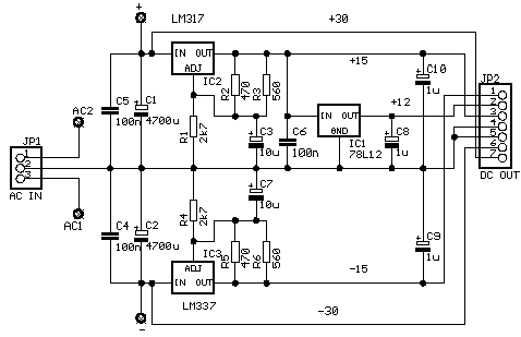
Power Supply
The power supply must produce the following voltages:
- +/- 30V (unregulated) @ 2A
- +/- 15V (regulated, ripple-free) @ 0.5A
- +12V (regulated) @ 0.1A
I made use of a 25-0-25, 200VA transformer, with an auxiliary 12V winding. (E-I design, not toroid, but you can use toroids if you can find them). The 25-0-25 AC is brought onto the board and rectified with a bridge rectifier (not shown). I made use of a small bridge rectifier board (these are available at Kwality electronics), which take in 1N5401 3A diodes. These can easily handle the power requirements of this project. Similar-power moulded bridge rectifiers would cost twice as much. This explains why the bridge isn't actually shown in the schematic, it's just shown as 4 points marked AC1, AC2, + and -. These are where the rectifier board wires are soldered in. The fullwave rectified DC is smoothed using two 4700uF, 50V filter capacitors.
Two 100nF capacitors shown are to be mounted close to the regulator ICs (LM317/337). I chose to use the more expensive LM317/337 over the 7815/7915 fixed regulators since the former have a much higher ripple rejection. This is because the reference voltage is smoothed out by C3 and C7. C4 and C5 help stabilize the regulators. R1, R2 and R3 form the voltage-selection network for the LM317. R4, R5 and R6 do the same for the LM337. The LM317's output is also used to power the 78L12 regulator to provide the +12 output. This regulator, too, has decoupling capacitors. These must be mounted close to the chip. C8, C9 and C10 are 1uF tantalum bead capacitors which provide good transient response for the regulators, and since they are tantalum caps, act as noise filters. Please note that tantalum caps are reported to be unreliable, although I've not had problems yet. For extra safety, insert a pair of 3A slow-blow fuses between the filter capacitors and the rest of the circuit (this includes the +/- 30V output and the +/-15V regulators)
 Warning: AC mains voltages are lethal. Exercise extreme care while soldering and testing, make sure all points exposed to AC mains are insulated using heatshrink rubber tubing. I am not responsible for accidents that may occur during construction, testing or useage of this circuit.
|
The transformer's AC side has a DPDT switch (the kind that have an inbuilt pilot lamp), 5A fuse (slow-blow recommended, although I couldn't find them; nobody seemed to know what slow-blow meant) and an MOV (varistor) across the transformer primary. Be absolutely sure to insulate ALL terminals, leads and wire exposed to the mains voltage.
 (Aug. 6, 2002) I found that Cee Pee electronics, Bangalore (see my Where to buy Components page) sells Slow-Blow fuses, although they're much more expensive than regular fuses.
|
Note that the total output voltage of this power supply is nearly 65V DC. This is a dangerous voltage to begin with, so don't touch the circuit while it's powered up. In addition, the 4700uF capacitors, when fully charged, have an energy of nearly 3 Joules each. This is a potentially dangerous amount of energy, so exercise caution. This much energy can melt the tip off a screwdriver used to short the output!
Fan Controller
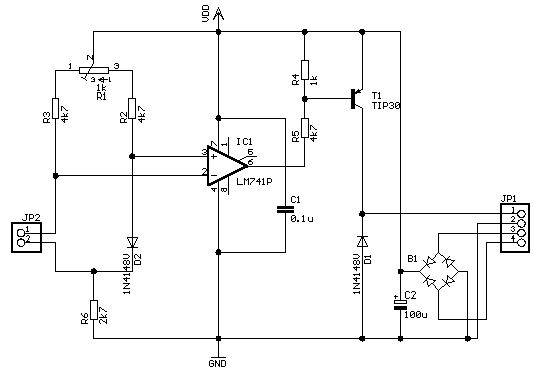
Fan Controller
The amplifier gets quite hot while in use, so decided to use a fan to cool it. The fan, however, adds a lot of noise. To get the best of both worlds, I thought I'd turn the fan on only when required. The circuit shown uses two forward-biased diodes, one as a sensor diode (at JP2) and the other as a reference diode (D2). The small difference in forward voltage drop is amplified by IC1 and used to drive T1. T1 turns on a fan when the temperature on the reference diode exceeds that at D2. D1 prevents inductive kickback from killng T1. B1 and C2 provide a rectified, regulated supply from the transformer's auxiliary 12V winding. This prevents noise from the fan motor getting coupled to the rest of the amp.
R1 is used to adjust the temperature cutoff point. This is done by first adjusting it to remain permanently off (turn it both ways, whichever way causes it to turn off, turn it all the way there). Now let the amp run for a while at a reasonably loud volume, so that the output devices heat up. Now place the reference diode on the heatsink of the output devices and back down R1 until the fan just turns on. Make sure that the fan is positioned such that after a while, it cools down the output devices enough to turn itself off.
This and the next circuit are built on the same board, and use the same auxiliary 12V supply, to avoid loading the 78L12 and to prevent fan noise from being coupled into the amp.
Speaker Protection
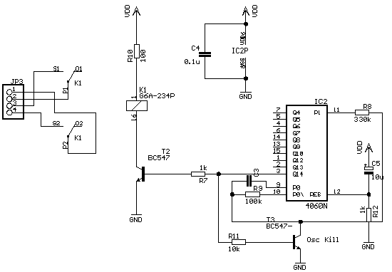
Speaker Muting
This is a simple delay circuit based on the CD4060 14-bit counter with an inbuilt RC oscillator. This oscillator is configured for a freqency of 4.5kHz using R=100k, C=0.001µF. The output at Q14 (divided by 212) is used to turn on T2 and T3. T3 kills the oscillations by shorting the timing capacitor to ground. This prevents Q14 from going low after it's period gets over. T2 turns on a relay, whose contacts enable the speaker leads. Thus, any click sound at turn-on is prevented. The 4060 is reset at power-on using the RC network R12/C5. I've inserted R10 in series with the relay because my relay had a 5V coil, if yours uses a 12V coil, omit R10. C4 decouples the supply to IC2.
Construction
Each subsection's schematic was entered into EAGLE PCB CAD software. I designed a board for each, with a 100mil (0.1" grid) and built the board on a piece of veroboard (prototyping board), as mentioned in my
PCB techniques page. The power supply distribution is done through a terminal strip, from which each board taps off it's power. Interconnections are through Relimate Connectors (RMCs). Signal interconnections are through shielded cable, but the shield was grounded only on the source side of the cable. This prevents ground loops.
All mains connections are insulated using heatshrink rubber tubing. This is not only more reliable than using insulation tape, but looks better and is less messy in case the joint needs to be broken. An DPST mains-rated switch (with a plastic, NOT metal body) is used to switch the mains supply. A slow-blow 2A fuse in series with the live (hot) mains lead provides protection in case of internal wiring faults, transformer insulation failure and power supply filter cap shorts.
The whole works is put into a ready-made metal (steel) chassis. Some metal work is needed to make the holes for the fan, input connectors, etc. My requirements were simple, and I made the front panel out of a sheet of "hardboard" (used to make photo frames, etc).
The Result
After struggling with some issues like getting the metalwork done on the cabinet, I finally managed to put the mixer together. It performs well, except sometimes when one of the amplifiers becomes unstable and bursts into oscillation. When I designed the circuits, I didn't consider capacitive loading, this might be what caused the oscillation. Capacitive loading at an amplifier's output can cause it to oscillate because the output stage is unable to control the feedback point fast enough to keep the error voltage zero. One easy way to avoid this is to use a damping resistor, of 100 ohms or so, at the output of all amplifiers which drive capacitive loads, such as coaxial cable.
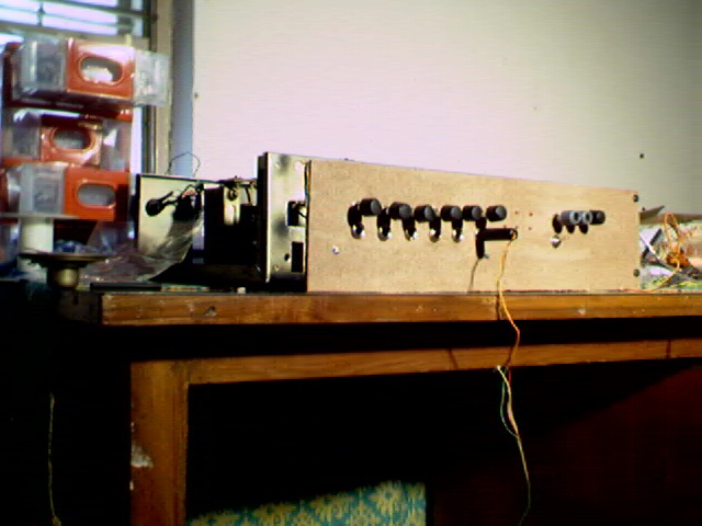
Outside view of the Mixer... note the really ugly construction.
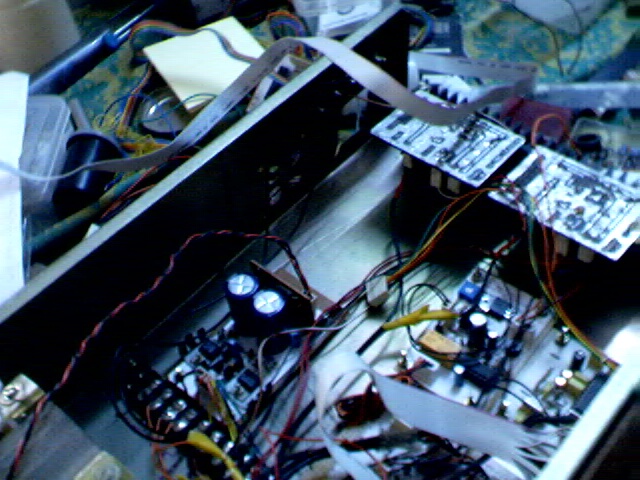
Inside view of the Mixer.
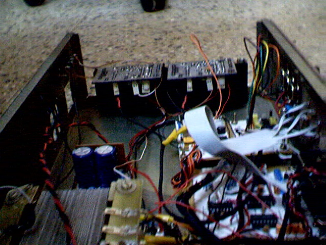
Another Inside view of the Mixer.
Disclaimer
These circuits are provided for your own study only. They all deal with electricity and electronics, a sufficient knowledge of both is assumed. I will not take any responsibility for any personal injury or damage to property arising from use or abuse of the information provided on these pages.