DSBSC Modulator and DPSK Demonstrator
One of the experiments in Communication Lab was to produce a DPSK modulated signal. For this, of course, we need a product modulator (PM). In our lab, we weren't expected to build the PM ourselves, rather, to use a kit available in the lab. This kit is an implementation of the circuit given in the LM1496 Balanced Modulator IC's datasheet, which has 51Ω termination resistors at both the inputs. This gives a very low input impedance which cannot be driven by a logic gate or opamp. Hence, I re-did the circuit with different termination resistors and a different carrier-nulling system. In addition, a signal symmetry adjustment is also provided. Keep in mind that this circuit is meant for AF use, and will not handle RF carriers (primarily due to the opamp).
Overview
The circuit can be broken into two parts, the DSBSC (product) modulator, and the digital waveform generator. The digital waveform generator uses a 4-bit shift register (7495) to produce a length-15 pseudorandom binary sequence (PRBS). This sequence is then differentially encoded making use of a D-flip flop (74LS74) and an XOR gate (74LS86). One of the 74LS86's gates is also used in the PRBS generator. The second part is the DSBSC modulator and amplifier. The modulator is based on the LM1496 balanced modulator. National Semiconductor has discontinued this chip, but Motorola still makes it, the MC1496P. The output of this chip is differential. Rather than taking one output alone, I made use of an opamp in a difference amplifier configuration to get a single-ended output. The gain is quite high, because the output of the LM1496 is a small voltage.
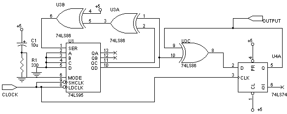
PRBS Generator
The PRBS generator is wired in a maximal length configuration, but the feedback loop uses an XNOR gate. One of the XOR gates is wired as an inverter, giving the XNOR action. All PRBS generators have a "forbidden state" into which if they fall, they cannot get out of on their own. If an XOR gate is used, this state is "0000". Using an XNOR gate, however, the state is "1111", which is less likely to occur due to noise, etc. The 7495 has a serial input, parallel synchronous-load inputs and a serial input. It has a MODE pin to choose whether the device is in serial mode (MODE = 0) or parallel load mode (MODE = 1). The clock inputs are seperate for different modes, but are tied together in this circuit. An RC circuit formed by R1 and C1 provides a power-on reset function for the shift register. This is done by momentarily putting the shift register in parallel load mode, which loads the value at ABCD into the shift register.
The differential encoder is based on a flip flop, which acts as a memory device to store the previous output, and an XOR gate, which acts as a mod-2 subtractor. For each new input, the output is the difference between it and the previous output. Hence the digital signal is differentially encoded.
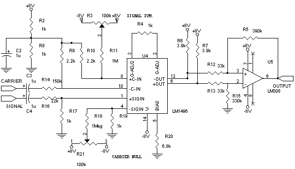
DSBSC Modulator
The DSBSC modulator is based on the LM1496 balanced modulator IC. This IC is quite unlike others used in various projects in that this IC resembles those made in the early days of IC fabrication, in which an IC contained little more than an array of transistors and most of the biasing, etc. had to be taken care of by external circuits. Nowadays, opamps and other linear ICs all have their own internal biasing mechanisms, which make them easy to use. Hence, it is rare to find projects on the 'net using this chip. The internal working can be understood by looking at the internal circuit diagram presented in the datasheet, available at
National Semiconductor's website. Most of the resistors in the circuit are used to set the bias point.
Note in particular, the two pots R3 and R21. These are used to set the signal symmetry and carrier nulling, respectively. In the ideal case, if the carrier frequency is fc and the signal frequency is fm, then the output has two components at fc - fm and fc + fm. However, some part of the message and carrier can feed through to the output. These controls are used to eliminate this effect. Carrier nulling removes any fc component, while message symmetry removes fm component.
The opamp forms a difference amplifier, which finds the difference between the differential outputs of the 1496 IC. Thus, any common mode signal (such as message signal feedthrough) will be completely eliminated. Unfortunately, the opamp limits the operating frequency of the circuit. To make use of a similar circuit at RF, you can use a transformer with a center-tap. The center-tap connects to the supply voltage and the ends go to pins 12 and 6 of the LM1496. I've not tried this myself, though. The opamp used is not critical, any opamp will do. I happened to have an LM308 lying around.
After constructing this circuit, I tested the DSBSC section first with two sine waves, and it worked as predicted. Next, I tried to make the carrier a music signal from a CD player, and the message signal an LF sinewave (< 300Hz) and got some really cool sounding effects! Try this with your own voice, it'll be hard to recognize! This may be used as the basis of a telephone security system. I also tested it with the DPSK signal and it worked as expected. With proper carrier nulling and message symmetry adjustment, the output looked textbook-perfect.
Corrections:
The 74LS95 shift register has an active-low clock, while the 74LS74 flip flop has an active-high clock. Thus, one of them should have an inverted clock, otherwise the differential encoding section will not work correctly. The unused XOR gate from the 'LS86 can be used for this. If you use a 74LS195 instead, this wont be necessary, since the 'LS195 has an active-high clock. This is probably a better solution, since I couldnt easily find 'LS95 chips. Drive the CLR pin with an RC circuit, to force it to a 0000 state at power up.
Disclaimer
These circuits are provided for your own study only. They all deal with electricity and electronics, a sufficient knowledge of both is assumed. I will not take any responsibility for any personal injury or damage to property arising from use or abuse of the information provided on these pages.