Circuit Construction Techniques
This is a description of how I currently implement circuits. These may not be the best ways to build circuits given the circumstances, but it works for me. Other methods (not covered here) include the
dead-bug style, Manhattan style, etc. For more info on these, search for "dead bug style" using
the Google search engine. PCB etching too, has several methods, many of which are either out of reach or impractical for the average experimenter.
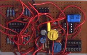
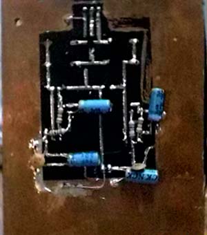
This mess was supposed to be
two fourth order chebyshev filters...
I used to build circuits on veroboard by first soldering the components, then using bits of wire on the component side to string them all up. This worked as long as the circuits involved carried only DC or low-frequency signals. "
Signal integrity? What's that???" As I progressed on towards building Audio circuits, noise was a problem. In any RF circuits I made, frequencies were unstable and output sometimes failed completely. High-speed digital circuits had noise pulses racing all over the circuit.
Pseudo-PCB technique
Eventually what changed me was during 6th sem project lab, when everyone complained that my circuits (which worked better than many others, I might add!) looked very untidy. If in doubt, just look at that picture :-) I found some pictures of circuits constructed using the dead-bug style and didn't like it one bit. Finally, the website "Electronics Beans Collection" (refer the links page) had a few nice pictures of circuits made on Veroboard that looked very professional, so I decided to try using component leads to make an approximation to PCB traces. I tried a few boards this way, but it was tough going to do the routing. Once I got the freeware version of the EAGLE PCB layout CAD software (from www.cadsoftusa.com), I could make proper layouts and print them out on paper. The constraint was that there had to be a 0.1" grid along which the component leads had to fall. This was done because the verobard I bought had a hole spacing of 0.1".
Both the signal layers are made use of, treating the bottom layer as the "pseudo-PCB traces" and the top layer as
wire-bridges on the component side.
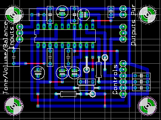
The EAGLE CAD layout of the board
Ah! Much better...
All routing is done by hand, using 0.05" traces. This ensures that there wont be any silly mistakes during the routing. Big components like ICs and connectors are aligned to the grid first (with the grid set at 0.05", but aligning to the 0.1" grid), and then all other components are placed. This ensures that you wont have to keep switching the grid size while placing components. Once the routing is done, select the bottom layer and the pads/vias and print it with a small zoom factor, with mirroring. This is the
wiring guide which is used in the next step. Next, print out the top layer and all the components, along with pads/vias at 100% zoom.
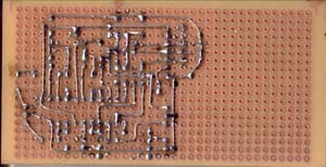
Component-side image
This is a
placement reference which is to be pasted using any ordinary glue onto the component side of the veroboard. Carefully align the placement reference (before pasting) such that the pads and vias align with the holes in the veroboard. Using a pin, punch small holes through the placement guide for each pad and via (the pin should fall through the veroboard hole). Do not use the component leads for punching the holes, as this will cause them to bend. First, solder all the wire bridges in place using stiff, single-core wire. The top-layer part of the component placement guide will tell you where to place the wire bridges. Next, using the component placement guide, insert the components into the veroboard and solder them in place. Snip off all the extra wire and save it for the next step. Remember to solder components in increasing height order.
Using a pair of nose-pliers, bend the component leads in the shape given in the wiring guide, and solder them in place. This takes some skill, and to ease the process, make sure the PCB traces during the layout stage are as simple as possible, with as few bends as possible. Once done, use a multimeter's continuity tester and check that there are no short circuits where there shouldn't be. Check all joints and power supply connections. You can do this easily by doing a "netlist check", for which you'll need a netlist. In EAGLE CAD, File->Export->Netlist should do the trick. Print out the netlist and verify the entire board pin-for-pin. For each verified connection, tick off the appropriate entry in the Netlist printout. Finally, connect the circuit's power and inputs, and verify that it works. Be the envy of all your friends when they see your perfectly crafted boards ;-)
Although it's a time-consuming method (because of all the time required to do the layout), it gives excellent results, and you dont run the risk of staining your life yellow (see below...) You can also make use of the snipped-off component leads, and not feel guilty that you're wasting them...
Inexpensive PCB Etching Technique
PCBs have always been my own personal Holy Grail, I've always wanted to make them on my own. Most online sources gave methods that involved using photoresist coating and UV exposure to make the patterns on the board. I've looked high and low for photoresist, and havent found it to date. Besides, if dust settles on the photoresist before it dries, it causes holes in the final PCB. Added to this is the "cooking period" under a UV lamp... basically way too much trouble for me. I was content with methods such as "Pseudo-PCBs" until I found out a way to make excellent quality PCBs without photoresist. It is called "toner-transfer" method, and involves transferring a pattern on paper onto the PCB, which acts as a mask during etching. I've modified it slightly, given that I dont have access to a drill and cannot drill holes through the PCB. The modification involves using a "surface mount" method: bend the pins of the components flat, and cut them short. Now solder them directly to the surface of the board, rather than first taking them through a hole. For ICs, please use the inexpensive type of IC socket, with thin, flexible leads. It would be very difficult (and wasteful) to use turned (machined) pin sockets for this application.
First, start with a PCB layout. The layout should be on a single layer, with pads visible. You can use the EAGLE layout editor to make the layout. Unlike the previous method, you aren't restricted to a 0.1" grid and don't have to try too hard to make a simple layout. In fact, you can even get away with using the autorouter. In EAGLE, set the costs for the component side layer to a high value (say, 30) to force most of the wiring to the solder side. The component side wiring can be done with wire bridges. Of course, this means you will have to manually drill holes for the vias. The layout is then printed mirrored onto a sheet of paper using a laser printer. If you don't have access to a laser printer, print it using an inkjet printer and photocopy this with the copier's intensity set to a dark value. Be sure that there is no dust on the copier's bed and that no zoom/reduction is used.
The copper clad (blank PCB) must be cleaned prior to etching. This is done using a wire brush; a coarse brush initially, and a fine brush after that. The brush is rubbed using circular movements so that the oxide buildup on the copper, along with any protective coating that may be applied, is removed. Finally, clean the board with a piece of cotton soaked in isopropyl alcohol (IPA). From this point on, do not touch the copper-side of the board with your fingers. Grease from your fingers can cause the etchant to not dissolve the copper under the oily area. Lay the photocopy/laser printout on the copper side, and trim it to size. Make sure the trace is aligned correctly with the board. Secure the paper onto the board using a small dot of glue on the non-solder side of the copper clad. Now press down on the paper with a clothes-iron set to it's highest temperature (the Linen setting, usually). Remember, no steam!!! Press down hard, and make sure that all parts of the copperclad are evenly heated. Continue heating for about 2 minutes, which is enough time to melt all the toner on the paper. Now cool the copper clad by holding it under water (use tongs or an oven mitten to pick up the hot board).
When cooled, the toner sticks to the copper clad as well as the paper. You now have to soak the board in warm, soapy water for a few minutes to allow the paper to get completely soaked. Once it is completely soaked, carefully peel away the paper without disturbing the toner on the copper clad. You will now have a perfectly masked board. You can use the fine wire brush to remove any small pieces of paper that may still be sticking to the toner. Dry the board (you can use a hair dryer) and once again clean it with IPA.
 Disclaimer: PCB etchants are hazardous, corrosive chemicals. Exercise extreme caution while using them. Wear eye protection and thick rubber gloves. Do not hold me responsible for any accidents that may occur while etching PCBs
|
Now comes the hazardous part: etching. You need a suitable etching tank. This must be made of a non-metal (ideally, plastic. Glass can break, flooding your work surface with corrosive chemicals). The tank must be big enough to lay your board flat in, and high enough to allow you to shake the tank gently without spilling etchant.
First, protect youself using rubber gloves and goggles. Next, choose your work area carefully. This should be in a draught-free room, with as few metallic objects around as possible (they can get corroded even by the vapour). Cover the area with newspaper and secure it such that uninformed people, children and pets cannot enter.
The etchant I use is Ferric Chloride. This is the most common and cheapest etchant, and gives reasonably good results. It comes in two varieties, anhydrous (dark green, crystalline powder) and hydrated (orange-brown, damp powder). Using the anhydrous version requires extra caution, as adding it reacts with water in an exothermal reaction, producing enough heat to boil the water. Hence, never add water to the powder, always add the powder to an excess quantity of water. Hydrated etchant is not nearly as dangerous, but it is just as corrosive. Dissolve 500gm of the powder in 1 litre of water (scaled down appropriately, it's unlikely you'll need that much etchant) and fill this in the tank. To improve the etching speed, add a little salt in the solution, and use warm water. Make sure there is some way to hold the board without exposing yourself to the etchant (use a piece of string or transparent tape). Stand the board in the etchant bath, being careful not to allow any air bubbles to stick to the board surface.
You'll immediately notice the un-masked copper surface of the board turns a "dirty brown" colour... this is the etchant at work. Soon, however, a layer of sludge forms on the surface, which must be removed. This is done by gently rocking the etching tank from side to side. If you want a better method, use an old aquarium pump to blow a steady stream of bubbles over the board surface. In this case, however, you'll want to keep the board inclined at an angle. Periodically verify that the board is done by checking to see if the unmasked copper has been completely eaten away.
Once the entire unmasked copper has been etched, remove the board and wash it under running water. Be careful not to allow the etchant to fall on any metal taps/fixtures. If you have any alkaline solution (KOH/NaOH), wash the board in a mild alkaline solution to remove all the etchant. Now use the fine wire brush and some paint thinner to remove some of the toner. Without paint thinner, it's very hard to get the toner out, since it's quite a tough material. Do not be too forceful while rubbing away toner, since you can remove the copper tracks along with the toner. Use a pen-knife to carefully scratch away any stubborn pieces of toner. At this stage, you can drill holes if you have a drill. Some components such as large diodes cannot be soldered using the surface mount method, hence you must drill holes. I do this using the reamer blade of a Swiss Army Knife.
Once all the toner is removed and the traces are in shiny, new copper, coat all the traces with soldering flux. Heat your soldering iron and melt some solder onto the tip. Spread this solder onto the traces. The solder will spread and stick to the board because of the flux. This 'tinning' process protects the copper from further corrsion as well as improves the conductivity of the traces. Components are now soldered using the "surface mount" method: bend the pins flat, parallel to the board surface. Cut them so that there is just enough lead to solder onto the pad. Cover the pin with flux before soldering, to ensure a good joint.
I dont have pictures taken during each stage of PCB production, I will try and make those next time I make a PCB. For now, here are two pictures of a finished PCB, a dual voltage regulator board.
 Bottom view - note the surface-mount capacitors and resistors. Also, the traces are tinned.
|
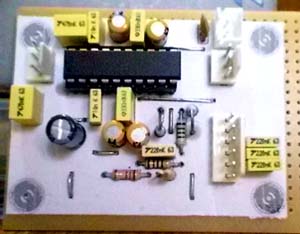
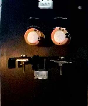 Top view. The two regulator chips are mounted through-hole, along with connectors and diodes.
|
One thing to remember with this method is that in case some of the components are surface mounted and some are mounted through-hole, the orientation must be correct. PCB software has no idea that you're planning to surface mount half the components, and will not compensate for this. Usually, this only matters when you're dealing with ICs, transistors, etc. One way to deal with this is to use the top layer of the board-layout software to design the layout, while using the bottom layer for wire bridges. Now, you can safely mount normal DIP chips and transistors, etc. on the solder side without getting their orientation wrong. The only shortcoming of this method is that all the ICs and transistors on a board must be on one side (ie, you cannot surface-mount some of them, while drilling holes for others).