Digital Voltmeter
This project was designed and built mostly for Technisium 2002, an electronics competition conducted by the Siddaganga Institute of Technology (SIT), Tumkur. Construction took about a week, including most of the software (ie, only a few features remained implemented). Afterwards, I got a PCB (four-layer) made, and the software was finished up. Later, I won second place for presenting the updated project at SJCE, Mysore during their inter-college competition, Cyberia 2002.
Overview
There are six major blocks in the device: The range selector, RMS-to-DC converter, ADC, microcontroller unit (MCU), keypad and LCD display. The range selector scales the input voltage down to a known value, under control of the MCU. It also includes protection circuitry, to prevent damage to the rest of the circuit in the event of a high voltage being applied with a low scale-factor selected. The scaled voltage is then fed to an AC/DC selection switch. This allows the MCU to choose either DC or true-RMS AC measurement. The selector's output is fed to the ADC's input. The ADC used is a MAX132 18-bit plus sign ADC with serial I/O. The ADC's output is read by an Atmel 90S8535 MCU, which does the required data formatting, conversion and storage functions. In addition, it implements the user interface via a 16x2 alphanumeric LCD, telephone keypad and an RS-232 link.
Schematic conventions
All analog power supplies are indicated by +5V, -5V and AGND. Digital power supplies are marked by Vcc and GND. Seperate power and ground planes have been maintained for these power supplies, and their interconnection will lead to poor noise suppression.
Analog Front End
The analog front-end pre-processes the input signal so that it is made presentable to the device's ADC. It has the following blocks:
Range Selector
This section is built around a CD4052 dual 4:1 analog multiplexer.
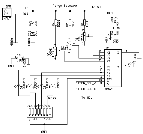
Range Selector
The range selector uses the voltage-divider principle to divide down the input voltage to a required value. The divider is formed by R10 along with one of the trimmer-resistor pairs (eg. R1 and R6, or R2 and R7). The trimmers are adjusted so that the voltages are then divided by a ratio 1:1 (if the mux is set to choose X0), 1:10 (if the mux is set to X1), 1:100 or 1:1000.
In addition, the zener diodes ZD1 and ZD2 provide protection against excessive voltage being applied, even if the divider does not provide enough attenuation. To understand how this works, assume the input voltage is 70V and the divider is set for a ratio of 1:10, giving an output voltage (on node AIN) of 7V. This is higher than the supply voltage of the internal ICs, and can cause failure. However, ZD1 and ZD2 clamp this down to their zener voltage, preventing damage. This works because there will always be a 1M resistance in series with the input voltage.
The second half of the multiplexer (which shares the same select lines) is used to form a range indicator, using four LEDs which are selectively grounded. Note that the method of using a SIP pack of resistors is wasteful, since only one LED can be lit up at a time. A single resistor between pin 3 of IC4 and +5V will do.
True-RMS to DC converter
This section is based around Maxim's MX536 RMS to DC converter chip and a buffer opamp (OP-07 low-drift opamp). This chip uses something called the "implicit method" to convert an AC signal to a DC voltage representing the AC signal's RMS value. Direct methods (such as heating up a wire and measuring it's temperature) suffer from inaccuracy and dynamic range limitations. The device's input impedance is rather low, hence I've used an OP-07 instrument-grade opamp to buffer the signal. This has the advantage of not requiring offset nulling (well, not much, anyway!). The signal is AC-coupled (through C6), otherwise the MX536 will also convert any DC offset.
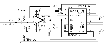
True-RMS to DC converter
The converted signal (node RMS_OUT) is fed to the coupling-mode selector. A dB scale output is also available at pin 5 of the chip. This can be buffered and fed to the coupling mode selector, which along with a few software changes can allow dB-scale measurements. I rather stupidly did not think of this before I made that PCB...
Coupling mode selector
The coupling mode selector allows the MCU to choose whether the ADC measures DC or RMS AC voltage. It's a straightforward section, based on the CD4052 dual 4:1 analog MUX.
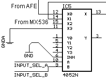
Coupling Mode Selector
Pin 13 goes to the ADC's input pin
ADC
Voltage Reference
The voltage reference section is based on the MAX872 voltage reference, which produces a 2.500V reference voltage.
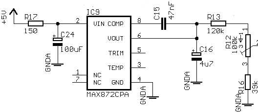
Voltage Reference
Supply voltage to the reference chip is heavily bypassed with a 150E resistor and 100uF capacitor, isolating it from potential digital noise voltage. The 47nF compensation cap is the manufacturer-recommended value. A 4.7uF tantalum capacitor at the output serves as an additional noise canceller. A potentiometer (R12) is used to divide the 2.500 V reference output to 512mV, the recommended full-scale range of the MAX132 ADC. Thus, R12 is the primary calibration adjustment.
ADC
The ADC uses the MAX132 18-bit plus sign multislope ADC with serial interface. This offers a very high resolution measurement capability, but is also highly susceptable to noise. Thus, power supplies must be carefully routed and bypassed.
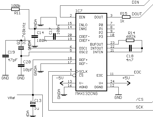
ADC
The ADC requires a reference voltage (bypassed to AGND near the chip with a 1uF tantalum capacitor), 32kHz oscillator crystal with startup capacitors C19 and C20 (these values were determined experimentally, they may not work with your particular brand of crystal), integrator capacitor C18, which must be a low-leakage film type, Reference storage capacitor (also film type), and input conditioning circuit (R11 and C14). R11 and C14 were taken from the MAX132 datasheet (a must-read), but C14 is too large, IMHO. I've used a 10nF here.
The digital interface is formed by DIN, DOUT, SCK, CS and EOC. DOUT has a 1k resistor for two reasons, it serves to isolate the ADC from the MCU's noise, and it also isolates the ADC during an in-system programming (ISP) session, which uses the same pin on the MCU to which DOUT is connected.
I learnt most of what I need to know about the ADC by hooking it up to my printer port, and using a small QuickBasic program to clock commands to the ADC and read back data. The datasheet is a bit confusing in this regard, but after some trial-and-error, I got the decoding right.
MCU
Microcontroller
The MCU I used is one leftover from my
6th sem project, an Atmel 90S8535. It's a very capable MCU, providing 8 MIPS at 8 MHz, 32 I/O ports, SPI, 256 bytes EEPROM, 8k code space and allows C programming (via the ICCAVR, gcc for AVR or CodeVisionAVR C compilers). Come to think of it, something like a 16F877 or an 8051 derivative such as Atmel's 89S8252 may have done the job just as well.
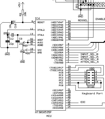
MCU, Keyboard port, Oscillator, part of LCD port
The MCU is provided with an 8MHz crystal (Q1) and startup capacitors C8 and C12. Power-On reset is through R9 and C10. Port A is used entirely for the LCD interface (an alphanumeric HD44780 compatible 2-line display), PA7-PA4 provide the data lines D7-D4 (I use the 4-bit interface), while PA1 gives the Enable pulse and PA0 provides the register-select signal.
Port B's upper nibble is used for communicating with the ADC (via SPI-bus) and for in-system programming (ISP). A 10-pin header is provided onboard to allow connection of an
STK-200 compatible programmer for firmware updates. The lower nibble of Port B is used to control the two multiplexers (range selection and coupling mode).
Port C is used for a keyboard connection. The lower four bits form the scan lines, while the upper four bits are the return lines. The keypad used is a spare meant to be used in a telephone. You must figure out the pin-outs manually, since they differ widely between keypad makes.
RS-232 link
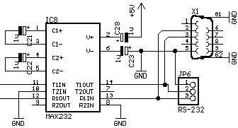
RS-232 interface
Port D is used for the RS-232 link (via an MAX232 level translator) and for receiving the EOC signal from the ADC as an interrupt on the INT0 line.
Power Supply
+5V supply
The power supply for the device is obtained from a modem power supply (a "Wall Wart" capable of supplying 9VAC @ 1A). Why AC? Well, modem adapters provide AC, and you can still use a DC adapter without problems.
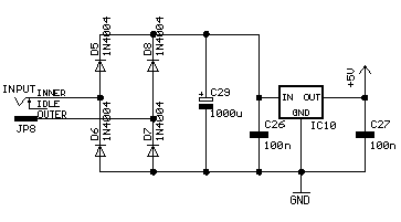
Power Supply
The input is rectified by D5-D8, smoothed by C29 and regulated by IC10, a 7805 three-terminal regulator. Space requirements can be reduced by using a packaged 1A bridge rectifier. Power supply diode switching noise can be eliminated by connecting 100nF disc ceramic capacitors across each diode in the bridge rectifier. The capacitors C26 and C27 must be disc-ceramic, and be mounted as close to IC10 as possible. Apparently, noise can be reduced by putting 0.1uF capacitors in parallel with the bridge rectifier diodes. This is supposed to reduce switching noise caused by the diodes. I've not noticed any difference.
-5V supply
The analog section of the DVM requires a -5V power supply in addition to the +5V supply. This is provided by IC3, an ICL7660 charge-pump voltage inverter.
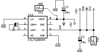
-5V inverter
Due to the switching action of IC3, it must be kept away from sensitive analog circuitry, and be on the digital ground plane. C2, C3 and C7 must be tantalum types, and lead-lengths should be small.
The Results
Here was one project that worked flawlessly the first time I switched it on! Perhaps it was because I had spent a long time with the MAX132 ADC, hooking it up to the parallel port, and writing programs to interface with it. Without that, I wonder how long the microcontroller program would have taken to write.
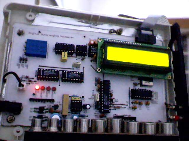
The pseudo-PCB version

The glorious 4-layer PCB version
The glowing LEDs are the range indicators. Text on the LCD was, uh, "eaten up" by the webcam I used. In the first picture, you can see the discarded modem case that I used to house the DVM. You can see quite a few changes in the PCB layout between the two; most of these were an attempt to move all the sensitive components (ADC, reference, input selector, amps, RMS converter) to one side of the board, and the noisy components (PSU, microcontroller) to the other side. Once seperated, the ground and power planes were split in two. The IC nearest the glowing green LED in the second pic is not incorrectly inserted, that pad had a short to ground (shrug...), so I had to lift the pin out of the socket. It drove the LED that's missing
Uday and I had put together a presentation for the SJCE Mysore competition. You can get the PDF version
here (467kB).
The DVM itself works very well, I managed to add autoranging, averaging, non-volatile reading storage, PC interface (via RS-232), min-max mode and a bargraph display.
Disclaimer
These circuits are provided for your own study only. They all deal with electricity and electronics, a sufficient knowledge of both is assumed. I will not take any responsibility for any personal injury or damage to property arising from use or abuse of the information provided on these pages.